Difference between revisions of "Making Parts for PCB Libraries"
| Line 1: | Line 1: | ||
{{guide| authors=Sasha Maldonado ({{slack-user|smaldonado}})}} | {{guide| authors=Sasha Maldonado ({{slack-user|smaldonado}})}} | ||
| + | |||
| + | {{Caution|1=This page is OUT OF DATE. Do not use it to learn how to do things!}} | ||
= WARNING!!! NO LONGER RELEVANT!!! = | = WARNING!!! NO LONGER RELEVANT!!! = | ||
Revision as of 01:57, 24 September 2020
 |
This is a guide Welcome! This article is intended to guide you through an SSI process. While its authors have made efforts to make it useful, if you have questions, please ask the authors on Slack. They will be able to both help you and improve this resource for future SSI-ers. This article was written by Sasha Maldonado ( |
|---|
WARNING!!! NO LONGER RELEVANT!!!
Altium 20 introduced a major change to the way libraries are managed. All of our libraries now live in the cloud, and there are no files on your computer associated with the libraries. You can still read this page, but it's an artifact at this point, so don't take it as truth. We are working on updating the Wiki, but for now ask in ![]() #altium
#altium
This article describes how to create a new part in SSI's Altium PCB component libraries. SSI maintains a collection of Altium component libraries, many of them derived from libraries generously donated to SSI by the Stanford Solar Car Project. This is designed to serve as both a reference, and a practical guide for how to turn a component with a datasheet into a schematic symbol with a corresponding PCB footprint.
This tutorial uses a template to show the keyboard shortcuts associated with certain tasks ![]() first key → second key → third key → etc.
first key → second key → third key → etc.
Introduction

Prior to creating a part, you should have installed and configured Altium and TortoiseSVN. In Altium, open the SSI Library project - SSI.libpkg, in SSI_SVN/libraries/intlib - with File → Open Project ![]() f → j
f → j![]() v → w → s → p
v → w → s → p
Altium has several different noteworthy types of libraries.
- Schematic libraries (.SchLib files) store schematic symbols and the components they correspond with. Schematic libraries contain schematic editor symbols, links to footprints (from PCB libraries; see below), mapping between the pins in the schematic symbol and pads on the footprint, and links to the part supplier (most often, Digi-Key)
- PCB libraries (.PcbLib files) contain the actual PCB layouts for library components. PCB libraries include footprints (the actual copper shapes and labels that will appear on the PCB) and 3D models of the associated packages.
- Integrated libraries (.LibPkg files) are Altium projects that combine schematic and PCB libraries.
- Compiled libraries (.IntLib files) are installable files that allow you to use library parts in schematics and PCBs. Every time a part is added to a library, the Integrated library will need to be recompiled before the part can be added to a PCB project.
For this tutorial, we will be mostly working with .SchLib and .PcbLib files. You will also need to open and compile the SSI.LibPkg file.
Locking in SVN

Prior to adding a part to a library, it's important to "lock" the library in SVN so that other people using the library don't create a conflicted copy. Locking does keep other people from making library edits at the same time, so do not lock a library unless you will be immediately editing it, and, even if a symbol or component is not completely done, commit any libraries you've locked before stepping away for an extended period of time (see Recompiling and SVN Management). To lock any library, right click on it in the Projects pane, click "Version Control," and then "Lock" ![]() right click → e → l
right click → e → l![]() #altium
#altium
What is a Part?
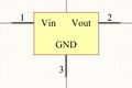
An example of a schematic symbol for an integrated circuit
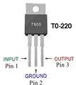
The above schematic symbol corresponds to this real part, which would have a footprint with three holes - one for each pin.
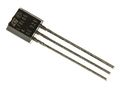
The above schematic symbol could be copied to refer to this part as well, because it has the same number of pins and each pin serves the same function.


A part represents a real electronic component - a resistor, a connector, an integrated circuit, etc. A part is defined in Altium with a couple of things:
- A schematic symbol - a symbolic representation of the part which doesn't have to look like the actual, real-life part but should show how to electrically connect to it.
- A footprint - a drawing that shows what should appear on the manufactured printed circuit board. The footprint must match the dimensions for every feature of the part that will be soldered to the PCB, and usually also includes labels and a 3D model that help gauge how big the part is and how it's supposed to be installed.
- A supplier link - a reference to a vendor's page to sell the part, most often at digikey.com. These links mean that boards that use the part can automatically generate a cart of all of the parts on the board, making it easy to order the parts to assemble the board.
Every part has a unique schematic symbol in Altium, though similar parts often use the same drawings, with pins renumbered as needed. Every part in Altium also has a unique supplier link. Parts in Altium can use the same footprint, as they correspond to (usually) industry standard form-factors used for many different parts. There are thus many more schematic symbols than footprints.
Creating a New Schematic Symbol
Drawing a Symbol
To create a new schematic symbol, first find the relevant schematic library. Schematic libraries are sorted by function - i.e. power management integrated circuits (PMIC), diodes, etc. The table below serves as a reference.
| Library Name | What Parts Go In It | Notes |
|---|---|---|
| capacitor.SchLib | Capacitors (all kinds). | Many ceramic capacitors are stored separately in sscp.dblib (ask in |
| connector.SchLib | Connectors (all kinds). | Schematic symbol names should start with "CONN_". |
| diode.SchLib | Diodes (all kinds, including light emitting). | Note the type of diode in the symbol name ("LED_", "SCHOTTKY_", "ZENER_" - you don't need to include the word "diode"). |
| fuse.SchLib | Fuses (both permanent and resetable). | |
| ic_analog.SchLib | Integrated circuits for analog applications (op-amps, filters, etc.). | Note the general category of IC in the symbol name ("OP_AMP_", "FILTER_", etc.) NOT for analog-to-digital converters (see ic_data_converters below) |
| ic_data_converters.SchLib | Converting data from analog to digital or vice-versa (ADCs and DACs). | Begin the symbol name with "ADC_" or "DAC_" as appropriate. |
| ic_digital.SchLib | Digital integrated circuits i.e. logic gates. NOT for processors (see ic_processor below). | Begin the symbol name with the logical operation the IC performs ("AND_", "XOR_", etc.) where appropriate. |
| ic_interface.SchLib | ICs for connecting to standard communications interfaces i.e. CAN, Ethernet. | |
| ic_pmic.SchLib | Power management integrated circuits, such as switching converters, linear regulators (LDOs), and battery protection. | Begin the symbol name with the converter type/topology ("LDO_", "BUCKBOOST_", "BUCK", etc.) where relevant. |
| ic_processor.SchLib | Processors (all kinds) | |
| Inductor.SchLib | Inductors (all kinds) and transformers. | Begin the symbol name with "IND_". |
| mechanical.SchLib | Mechanical features, such as mounting screws, and test features, like test points. | |
| miscellaneous.SchLib | Parts not properly described by any other category. | Use is discouraged, because it has a tendency to be a dumping ground - make sure there really isn't anything better. |
| modules.SchLib | Standalone modules i.e. prebuilt Arduino boards | |
| Oscillator.SchLib | Oscillators and crystals. | |
| Resistor.SchLib | Resistors not available in resistor.dblib | All 1% resistor values in standard surface mount sizes are stored in resistor.dblib. Prefix the symbol name with "RES_". |
| rf.SchLib | Radio frequency parts and antennas. | RF connectors should stay in connector.SchLib |
| sensor.SchLib | Sensors (all kinds) | Prefix the symbol name with the kind of sensor ("ACCEL_", "GYRO_", etc.) |
| transistor_bjt.SchLib | Bipolar junction transistors. | We have mercifully few of these. |
| transistor_fet.SchLib | Field effect transistors (all kinds). | Please note polarity by prefixing with "NFET_" or "PFET_" as appropriate. |


Next, lock the library you'll be working with, and double click the library to open it. If not already visible, open the "SCH Library" pane ![]() v → w → c → b
v → w → c → b
Next, you'll draw out the graphics for your symbol. Begin by setting the snap grid of the editor (the grid of points it will allow for drawing) to 10 point spacing, by opening the snap grid settings ![]() v → g → s
v → g → s
For logic gates, transistors, and other components that traditionally have distinct schematic symbols, it is helpful to draw those symbols - you can often copy the graphics from an existing, similar part by simply opening the existing part from the symbols list in the SCH Library pane, selecting all of the symbol in the editing window and copying, then reopening and pasting into your own symbol. You should then delete all of the pins and replace them as described below. If no suitable symbol exists, draw a symbol by placing lines ![]() p → l
p → l
Integrated circuits are typically represented in schematics simply with rectangles; you can place a rectangle ![]() p → r
p → r
Pins
Pins are how your symbol will be connected to wires when used in schematics. Enter the pin placement tool ![]() p → p
p → p![]() tab
tab![]() tab
tab
Next, resize rectangles and lines and move pins around until you're satisfied with the look of the symbol. You're done drawing the symbol! Make sure to save the .SchLib you're working on - if you're not going to immediately proceed to Creating a New Footprint and/or Finishing a Component, commit the library you were working on - this will release the lock and allow others to work on the library.
While this is the generic approach for drawing a schematic symbol, Altium also contains tools for automatically drawing certain types of symbols.
Creating a New Footprint
Footprints are the geometries of the actual layers that will be made on a printed circuit board. They correspond to the "packages" components come in - ie. SOIC, SOT-23, and many more - and so are often reusable between different components. While schematic libraries were sorted by function, footprints are sorted by series (QFN, DFN, etc.) and part type. If the package type marked on your component's datasheet doesn't clearly fit a series and isn't a passive (resistor, capacitor, or inductor) and isn't a sensor (appropriate if the symbol was made in sensor.SchLib) or module (i.e. a full microcontroller, like a Teensy board), it probably belongs in the Miscellaneous library.
As before, lock the library your footprint will be added to, then open the library. If not already visible, open the "PCB Library" pane ![]() v → w → p → b
v → w → p → b
The component you created a symbol for above may already have a footprint in a PCB library; search for it before starting work in the next two sections, and if it exists, skip to "Finishing a Component".
IPC Compliant Footprint Generator

If your component is a standard package, there's a good chance you'll be able to generate your footprint using Altium's IPC Compliant Footprint Generator. Open up the tool ![]() t → i
t → i
Drawing a Footprint
If the IPC Generator isn't an option, you can place pads manually ![]() p → p
p → p![]() tab
tab
When placing a pad, first set the designator to indicate what pad you're placing. The designator does not have to be a number, and should match the designator of any schematic pin it will be connected to. Multiple pads with the same designator''can''be placed, and will all connect to the relevant schematic pin. This is useful for creating a polygonal pad shape out of several rectangular pads, as well as components where a single electrical net connects to multiple physical pads - for example, a Teensy board, which has multiple identical GND pins.
After setting the designator, set the layer of the pad. "Top Layer" pads are surface mount pads (and will have their copper exposed appropriately); "Multi-layer" pads will expose copper on both sides of the board, and can thus have holes put through them. If making a multilayer pad, check off "Plated" - failing to do so will trigger errors and cause your through holes to just be... well, holes. Finally, set size and shape accordingly, and hit okay to return to placing your pad. One option is to place your pad where it needs to go - the current coordinates of your mouse and snap grid size and units are displayed in the upper left, and you can freely change the units ![]() q
q![]() v → g → g
v → g → g

Optional but very strongly encouraged: One of the strengths of the SSI PCB libraries - and a special feature of Altium - is the use of 3D models for 3D renders of PCBs. Search online for a STEP file for your component; while far from guaranteed, many components have models freely available. If possible, download one. To insert it into your footprint, use the Place 3D Body tool ![]() p → b
p → b![]() 3
3![]() 2
2
Finally, using the line tool ![]() p → l
p → l![]() p → u
p → u
Finishing a Component
Pairing Schematic Symbols and Footprints

After finishing a schematic symbol and footprint, switch to the schematic symbol in the schematic library editor. In the "Editor" pane at the bottom of the screen, click "Add Footprint," then "Browse." From there, find the relevant PCB footprint library in the dropdown, and then the relevant footprint within the library. Double click the footprint to return to the "Add Footprint" dialogue, where the selected footprint's details will now be shown.
Click "Pin Map," and confirm that the pins on the schematic symbol match up appropriately with the pads on the footprint (if pins were given designators that correspond with their pad numbers, this should have happened automatically). If they don't match, edit the fields until they do. Multiple schematic pins can map to the same footprint pad, but not the other way around - for two pads to connect to the same pin, they must be given the same number in the PCB library editor.
Next, click OK. Your schematic symbol is now paired with a footprint! The footprint should now show up in the list of footprints at the bottom of the Editor pane.
Adding Supplier Links

The final step is to add a link to a supplier part, to allow for automated BOM ordering. Open the "Supplier Search" pane ![]() v → w → s → u
v → w → s → u![]() v → w → c → b
v → w → c → b
You're done creating this component! Save the schematic library, and proceed to the final steps below.
Recompiling and SVN Management
Recompiling the Integrated Library
Before you can use your new part, you'll need to recompile the SSI library. Recompile using ![]() c → c
c → c
Commit Files to SVN
Committing files to the SSI Altium SVN is important for synchronizing files across users. Proper locking is required to keep commits simple and easy. If you've changed a single file, right click the changed library in the Projects pane, click "Version Control," and then "Commit" ![]() right click → e → c
right click → e → c
You will be prompted for a commit message; describe the changes made in at least 20 characters. This minimum is imposed in an attempt to keep people from entering commits without useful messages. It's easy to get around this, but you'll be a better person for telling other people what you did. Your commit should then quickly complete, your version control state will update, your lock on the library will be released, and within 15 minutes your commit should be automatically posted to Slack. You are now, actually, finally, done - assuming your commit proceeds successfully. In the event of a failure, poke the ![]() #altium
#altium
There are several hundred parts in the whole Altium library, between the contributions of SSI and Stanford Solar Car members. The process you've just completed has been gone through many times - and you benefit from everyone who spent effort to do it correctly before you. You owe that same favor to the people who will use the library after you.